Lab #1: The AND Gate
The first lab was a simple circuit where an LED followed the AND Logic Gate. In other words, the LED would only light up when both inputs were set to high. In a schematic, it would look something like this:
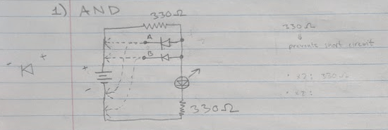
As shown, the inputs (A and B) can be moved to either positive or negative. If either one is moved to negative, then the power will automatically go through the diode and into the negative, taking the path of least resistance. However, with both connected to positive (meaning “1” or “ON” or “HIGH”), the power from the battery is forced to go through the LED, lighting it up. The two 330 resistors are to prevent a short circuit and fried LED.
Since this was my first lab, I didn’t quite think ahead enough to take a nice picture with a cute sticky note label, but I did make a video:
P.S. the waving at the end showing my ring (plus the to-do list with my distinctive profile picture) is just so my teacher knew it was me as proof!
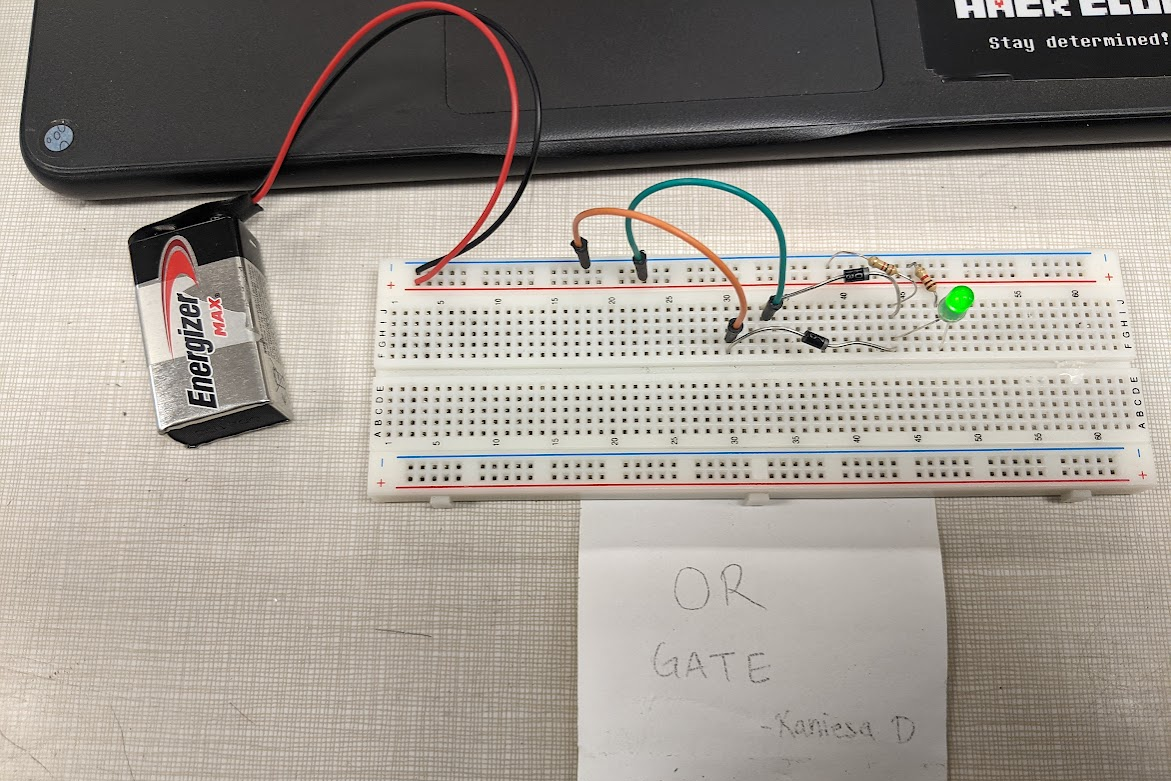
Lab #2: The OR Gate
This next lab was very very similar to the previous lab, and followed the OR Logic Gate. This means that if any input was connected to positive, then the LED would flash. (in other words, the only case where the LED would not light up would be is every input was connected to ground)
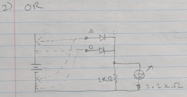
As shown, the inputs (A and B) can be connected to either positive or negative. If both inputs are connected to negative, then there is no connections to positive, meaning the power from the battery does not go anywhere, leaving the LED unlit. However, if even one input is connected to positive, then power will go through the entire circuit, lighting up the LED. As always, the resistor is to prevent a short circuit and fried LED. Although I did have an interesting discussion with my teacher as to where the second 1.1K resistor (running parallel to the LED) was truly needed.
Here’s a picture and video:
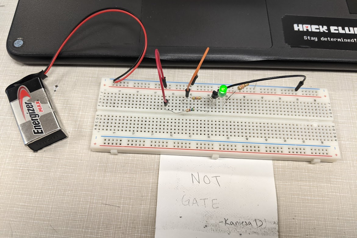
Lab #3: The NOT Gate
This next lab was slightly different from the first two, as it used a transistor for one input instead of two diodes for two outputs, in order to create the NOT Gate. A not gate produces the opposite output from the input. Here’s the schematic and explanation so it makes sense:
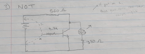
As shown, there is only one input (A) and if it is connected to positive, then the LED will not light up, but it is connected to ground, then the LED will light up. This is because the transistor is working as a switch so when the input goes to positive, the transistor allows the power to go through it, skipping over the LED. Otherwise, the power will not pass through the transistor, and through the LED, lighting it up!
As usual, here’s the final result media:
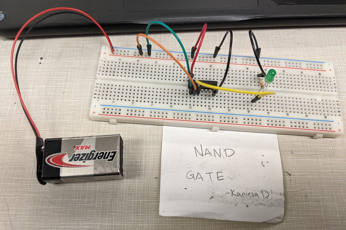
Lab #4: The NAND Gate
This final lab (of this post) is the most different from the previous ones as it introduces the 4011 Chip to create the NAND Gate Circuit. In this, the circuit works opposite to the AND Gate; the LED will light up in every condition that the AND Gate LED wouldn’t. In other words, the LED will always light up unless both inputs are set to positive.
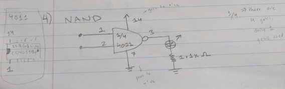
To be honest, the chip does most of the work as the 4011 is a chip with four NAND gates (NAND because it’s a universal gate). In this lab, only one of the NAND gates gets used, with pins 1 and 2 as our inputs. Pin 3 is connected to our output, where our LED and resistor are! Meanwhile, pins 7 and 14 are our negative and positive pins respectively.
As always, here’s the picture and video (apologizes for the shakiness of the video, I only had a minute until the bell rang):
Post-Labs Reflection
To conclude, I had a great time making these circuits. To be honest, I expected it me to take much longer than it did, which is why I was so happily surprised that I managed to finish all four of the first labs in one class period- which is an hour and fifteen minutes at my school! If you don’t believe me, check out the date and times in the videos above (I’ll admit that I the made the short time gap quite obvious by pridefully zooming in at the time in the last few labs).
I can’t wait to continue working on the labs!
Be back soon,
– K.D

Leave a reply to cristencarrion1984 Cancel reply